


Halfgeleiervervaardigingsfasiliteite werk onder die mees streng skoonheidstandaarde in moderne vervaardiging, waar selfs mikroskopiese besoedeling miljoene dollars se produk kan vernietig. In die hart van hierdie streng vereistes lê ultr suiwer water, 'n kritieke proseschemikalie wat deurlopend tydens skyfverwerking gebruik word, veral tydens spoelbewerkings wat tussen elke vervaardigingsstap plaasvind. Silikon-skywe, die fundamentele substraat vir geïntegreerde stroombane, moet met water gespoel word wat so suiwer is dat dit prakties geen opgeloste vastestowwe, organiese stowwe, deeltjies of mikro-organismes bevat nie. Die rede hoekom halfgeleierfabrieke ultr suiwer water vir die spoeling van silikon-skywe benodig, is die ekstreme sensitiwiteit van nanoskaal-toestelstrukture vir besoedeling, die behoefte om presiese oppervlakchemie te handhaaf, en die ekonomiese noodsaaklikheid om opbrengs te maksimeer in 'n bedryf waar 'n enkele defek 'n hele skyf nie-funksioneel kan maak.
Die halfgeleiervervaardigingsproses behels honderde opeenvolgende stappe, insluitend fotolitografie, etsering, afsettingsprosesse en ioonimplantasie. Na elke chemiese behandeling of fisiese proses moet skyfies grondig gespoel word om residuële chemikalieë, reaksiebyprodukte en deeltjies te verwyder voordat daar na die volgende stap beweeg word. Die gebruik van enigiets minder as ultr suiwer water bring kontaminante in wat aan skyfoppervlaktes adsorbeer, die volgende verwerkingsstappe versteur, die elektriese eienskappe van toestelle verander of defekte skep wat deur die res van die vervaardigingsreeks voortplant. Soos toestelgeometrieë onder tien nanometer krimp, word die toleransie vir onreinhede wat in dele per biljoen gemeet word, absoluut noodsaaklik. Om te verstaan hoekom halfgeleierfabrieke op ultr suiwer water staatmaak, vereis dit dat ons die kontaminasiemeganismes wat toestelprestasie bedreig, die gehaltestandaarde wat water suiwerheidsvlakke definieer, en die bedryfsgevolge van ontoereikende spoelwaterkwaliteit ondersoek.
Die Besoedelingskwesbaarheid van Silikonplaatjies Tydens Vervaardiging
Nanoskaal-toestelgevoeligheid vir Spoorimpuriteite
Moderne halfgeleier-toestelle beskik oor transistorhekke, interverbindings en ander strukture wat in enkel-syfer-nanometer gemeet word, wat 'n baie groot oppervlak-ten-op-volumeverhouding skep wat hulle buitengewoon kwesbaar maak vir oppervlakbesoedeling. Wanneer plaatjies met water gewas word wat selfs net 'n paar dele per miljard metaalione soos natrium, kalium, yster of koper bevat, adsorbeer hierdie besoedelings vinnig op silikonoppervlaes en migreer na hekgoxide of lasgebiede. Metaalbesoedeling skep mobiele ioniese spesies wat drempelspannings verander, lekkasie-strome verhoog, draer-mobiliteit verminder en toestelbetroubaarheid met tyd verswak. 'n Enkele metaaldeeltjie van net tien nanometer kan aangrensende stroombaanstrukture by gevorderde nodes verbind, wat kortsluitings veroorsaak of kapasitansiewaardes buite ontwerpspesifikasies verander. Die gebruik van ultr suiwer water voorkom dat hierdie metalliese kontaminante die skyfoppervlaktes bereik tydens die kritieke spoelstappe wat na nat chemiese prosessering plaasvind.
Organiese besoedeling stel halfgeleiervervaardiging ewe ernstige risiko's. Fotoretentiemateriaalrestante, oplosmiddelmolekules, oppervlakaktiewe stowwe en atmosferiese koolwaterstowwe kan dunvelle op skyfoppervlaktes vorm wat die volgende fotolitografie-stappe versteur deur retentiehegting te verander of defokusfoute te veroorsaak. Organiese molekules ontbind ook tydens hoë-temperatuurprosesse en laat koolstofagtige restante agter wat afsettingskamers besoedel of holtes in dielektriese lae skep. Bakterië, biofilms en endotoksine voer beide deeltjie- en organiese besoedeling in, terwyl mikrobiese groeiprodukte nanoskaalpatrone kan vorm wat oor skyfoppervlaktes herhaal word. Stelsels vir ultr suiwer water maak gebruik van verskeie tegnieke vir organiese verwydering, insluitend UV-oksidasie en geaktiveerde-koolstoffiltrasie, om totale organiese koolstofvlakke onder vyf dele per miljard te handhaaf en sodoende hierdie organiese besoedelaars daarvan te weerhou om toestelstrukture te kompromitteer.
Meganismes vir Defekvorming wat deur Deeltjies veroorsaak word
Deeltjiebesoedeling verteenwoordig een van die mees algemene opbrengsbeperkende faktore in halfgeleiervervaardiging. Deeltjies wat in spoelwater versprei is — of dit nou anorganiese minerale fragmente, neergeslagte soutkristalle of organiese rommel is — word op skyfoppervlaktes afgeset deur gravitasie-afsetting, elektrostatiese aantrekking of hidrodinamiese kragte tydens spoel- en droog-siklusse. 'n Deeltjie wat vyftig nanometer meet, kan 'n stroombaanfunksie in sub-sewe-nanometer prosesknoppe heeltemal blokkeer, wat oop stroombane of kortsluitingsdefekte veroorsaak. Deeltjies wat op fotorestis tydens litografie beland, skep gaatjies of patroonvervormings wat deur daaropvolgende etserings- en deposisie-stappe voortplant. Selfs deeltjies wat aanvanklik op nie-kritieke areas rus, kan tydens latere verwerking gemobiliseer word en na sensitiewe toestelareas migreer waar hulle latente foute veroorsaak.
Die uitdaging verskerp omdat deeltjies sterk oppervlakinteraksies met silikon en silikondioksied vertoon. Van der Waals-krigte, elektrostatiese aantrekking en kapillêre hegting tydens droë word maak dit moeilik om die deeltjies te verwyder nadat hulle afgeset is. Dit vereis dus dat die afsetting van deeltjies vanaf die begin voorkom word deur streng beheer van die kwaliteit van spoelwater. Stelsels vir die vervaardiging van ultr suiwer water sluit verskeie filtrasiestappe in, wat gewoonlik punt-van-gebruikfilters met poriegroottes tot tien nanometer insluit, wat verseker dat die aantal deeltjies onder een deeltjie per milliliter bly vir deeltjies groter as vyftig nanometer. Die herwinningseienskap van ultrasuiwerwatersisteme, met aanhoudende filtrasie en monitering, handhaaf hierdie buitengewone skoonheidstvl gedurende die hele bedryf van die fabriek.
Verandering van Oppervlakchemie en Probleme met Prosesintegrering
Benewens die inbreng van afsonderlike kontaminante, verander onzuivere spoelwater die fundamentele oppervlakchemie van silikon skyfies op maniere wat daaropvolgende vervaardigingsstappe kompromitteer. Silikonoppervlaktes vorm natuurlik 'n dun aangebore oksiedlaag wanneer dit aan suurstof en water blootgestel word. Die dikte, samestelling en kwaliteit van die grenslaag van hierdie oksied hang krities af van die suiwerheid van die water wat tydens spoeling gebruik word. Opgeloste ioonse in water, veral silikate, borate en fosfate, word in hierdie aangebore oksied ingevoeg, wat sy dielektriese eienskappe en etsspoedkenmerke verander. Wanneer skyfies met kontamineerde oppervlakoksiede in oonde vir termiese oksidasie ingevoer word of voortgaan na poortdielektriese deposisie, toon die resulterende lae nie-eenformige dikte, verhoogde grenslaagvalgrawwe-digtheid en gekompromitteerde elektriese integriteit.
Waterkwaliteit beïnvloed ook die waterstof-terminasie van silikiumoppervlaktes, 'n kritieke faktor in die voorkoming van oksidasie en die handhawing van oppervlakpassivasie. Na waterstoffluoriedsuurbehandelings wat natuurlike oksiedlae verwyder, word skyfies met ultr suiwer water afgespoel om residuë van fluoïedione te verwyder terwyl waterstof-geëindigde silikiumbindings bewaar word. Indien die spoelwater opgeloste suurstof, metaalkatalisators of ander oksiderende spesies bevat, breek die waterstof-terminasie vinnig af, wat lei tot onbeheerde oksiedhergroei en oppervlakruheid. Chemies-meganiese planarisasieprosesse, wat meganiese afskraap met chemiese etsing kombineer, vereis ultr suiwer waterspoelings om slurrydeeltjies en neweprodukte te verwyder sonder om die presies planariseerde oppervlak te verander. Enige ioniese spesies wat na die spoeling agterbly, beïnvloed die elektrochemiese potensiaal van die oppervlak en het dus gevolge vir korrosiegedrag en die eenvormigheid van daaropvolgende metaalafsettings.
Bepaling van Ultrasuiwer Waterkwaliteitsstandaarde vir Halfgeleiertoepassings
Weerstandsheid- en ioonbesoedelingspesifikasies
Die halfgeleierindustrie definieer ultrapuur waterkwaliteit deur verskeie parameters, waarvan weerstandsheid die primêre real-time aanwyser van ioon suiwerheid is. Ultrапuur water vir halfgeleiertoepassings moet 'n weerstandsheid van agtien komma twee megohm-sentimeter by vyf-en-twintig grade Celsius bereik, wat die teoretiese maksimum suiwerheid van water by ewewig met atmosferiese koolstofdioksied voorstel. Hierdie weerstandsheid stem ooreen met 'n totale ioonbesoedeling van minder as een deel per miljard, terwyl individuele metaalione gewoonlik tot sub-deel-per-triljoen vlakke beheer word. Die SEMI F63-standaard, wat deur SEMI (Semiconductor Equipment and Materials International) gepubliseer is, verskaf besonderde spesifikasies wat weerstandsheid, totale oksideerbare koolstof, deeltjie-tellings, bakteriële tellings en opgeloste suurstof insluit, en skep so 'n omvattende raamwerk vir ultrapuur waterkwaliteit oor die hele industrie.
Die bereiking en handhawing van hierdie buitengewone suiwerheid vereis voortdurende monitering en 'n veelstadium-behandeling. Bronwater, of dit nou munisipale versorging of putwater is, begin met totale opgeloste vastestowwe gemeet in honderde dele per miljoen. Voorbehandelingsfase soos multimedia-filtrasie, geaktiveerde koolstofadsorpsie en water-ontsoutting verminder groot hoeveelhede besoedelaars voor die primêre suiweringsproses. Omgekeerde osmosestelsels verwyder agt-en-negentig tot nege-en-negentig persent van opgeloste ioon, organiese stowwe en deeltjies, en produseer permeaat met 'n weerstand van ongeveer een megohm-sentimeter. Elektrode-ionisasie of gemengde-bed-ioonuitruiling as 'n afwerkingsproses volg daarna, om die weerstand te bring na die teikenvlak van agtien komma twee megohm-sentimeter. Ultrahuiwater word dan deur vervaardigingsareas gesirkuleer in geslote-lusstelsels met voortdurende hergenerering, wat konsekwente gehalte by elke gebruikspunt verseker.
Vereistes vir organiese koolstof- en mikrobiologiese beheer
Totale organiese koolstofspesifikasies vir ultr suiwer water vereis gewoonlik vlakke onder vyf dele per miljard, met sommige gevorderde toepassings wat suiwerheid van minder as een deel per miljard vereis. Bronne van organiese besoedeling sluit natuurlike organiese materiale in die bronwater, biofilmvorming in verspreidingsstelsels, uitspoeling uit pypmateriale en atmosferiese besoedeling by gebruikspunte in. UV-oksidasie-stelsels wat by agtien-en-tagtig en twee-honderd-vyf-en-tagtig nanometer golflengtes werk, fotooksideer organiese molekules na koolstofdioksied en water, wat daarna deur ontgassingmembrane en ioonruil verwyder word. Hierdie UV-behandeling verminder nie net die totale organiese koolstof nie, maar voorsien ook kontinue desinfeksie, wat bakteriële kolonisering van die ultrasuiwer-water-verspreidingsnetwerk voorkom.
Die beheer van mikrobiologiese kontaminasie stel unieke uitdagings omdat selfs dooie bakteriële selle en hul sellulêre fragmente skywe kan kontamineer. Lewende bakteriële kolonies kan minder as een kolonievormende eenheid per milliliter in ultrapuur water wees, maar die totale bakterietelling, insluitend lewende en nie-lewende selle, moet onder tien selle per milliliter bly. Bakteriële endotoksine, lipopolisakkariede uit gram-negatiewe bakteriële selwande, is veral probleemagtig omdat hulle selfs na die dood van die selle aanhou bestaan en die hegting van fotoretor kan versteur. Ultrapuurwatersisteme tree mikrobiologiese kwessies aan deur middel van UV-desinfectie, sanitasie-siklusse met warm water, membraanfiltrasie met absolute poriegroottes onder twintig nanometer, en materiaalkeuse wat biofilmvorming tot ‘n minimum beperk. Die ontwerp van die verspreidingslus sluit turbulente vloei-omstandighede in en vermy dooie vertakkinge waar stilstaande water mikrobiese groei kan onderhou.
Deeltjiegetalstandaarde en Metingsuitdagings
Deeltjiebesoedelingspesifikasies vir ultr suiwer water het dramaties verskerp toe toestelafmetings gekrimp het. Huidige standaarde vereis gewoonlik minder as een deeltjie per milliliter vir deeltjies groter as vyftig nanometer, met sommige kritieke toepassings wat opsporing en beheer van deeltjies tot twintig nanometer vereis. Die meting van deeltjies in hierdie groottebereik tree konvensionele vloeibare-deeltjie-teltegnologie uit, wat laser-gebaseerde instrumente vereis wat in staat is om ligstrooiing van individuele nanoskale voorwerpe op te spoor. Die halfgeleierindustrie gebruik kondensasiedeeltjietellers wat nanopartikels deur middel van beheerde oorsadurering na opties waarneembare groottes laat groei, wat akkurate tellings van deeltjies in die tien tot vyftig nanometer-bereik moontlik maak.
Deeltjies in ultrasuiwer water is afkomstig van verskeie bronne, insluitend onvolledige verwydering tydens behandeling, generering binne die verspreidingstelsel deur korrosie of materiaaldegradasie, en bekendstelling by gebruikspunte deur toerusting- of omgewingsbesoedeling. Gebruikspuntfiltrering verteenwoordig die finale verdediging, met vervaardigingsgereedskap wat terminale filters insluit onmiddellik voor kontak met die wafer. Hierdie filters, tipies vervaardig van politetrafluoroëtileen- of nylonmembrane met tien tot twintig nanometer poriegraderings, verwyder deeltjies terwyl ultrasuiwer watergehalte gehandhaaf word. Gereelde filtervervanging gebaseer op differensiële drukmonitering of tydsintervalle verseker konsekwente deeltjieverwyderingsprestasie. Die hele ultrasuiwer waterstelsel funksioneer as 'n geïntegreerde kontaminasiebeheerstrategie waar bronwaterbehandeling, verspreidingstelselontwerp en gebruikspuntfiltrering saamwerk om die vereiste deeltjieskoonheid te lewer.
Ultr suiwer Waterproduksietegnologieë en Stelselargitektuur
Ontwerp van 'n Veelstadiumbehandelingsproses
Die vervaardiging van ultrasuiwer water vereis 'n noukeurig gevolgde reeks behandelingstegnologieë, waarvan elkeen spesifieke kontaminantkategorieë aanpak. Die proses begin met voorbehandelingsfases wat die bronwater kondisioneer en die volgende suiweringsuitrusting beskerm. Multimediavilters wat lae van antrasiet, sand en graniet bevat, verwyder verspreide vastestowwe en troebelheid. Geaktiveerde-koolstofvilters adsorbeer chloor, chloramien en organiese verbindings wat omgekeerde-osmose-membraan kan beskadig of die klaar ultrasuiwer water kan besoedel. Waterversagters of anti-skaler-injeksie voorkom minerale afsettings op membraanoppervlaktes. Hierdie voorbehandelingsstappe verminder die kontaminantbelasting met negentig tot vyf-en-negentig persent, wat die leeftyd van die daaropvolgende suiweringsfases verleng en die algehele stelseldoeltreffendheid verbeter.
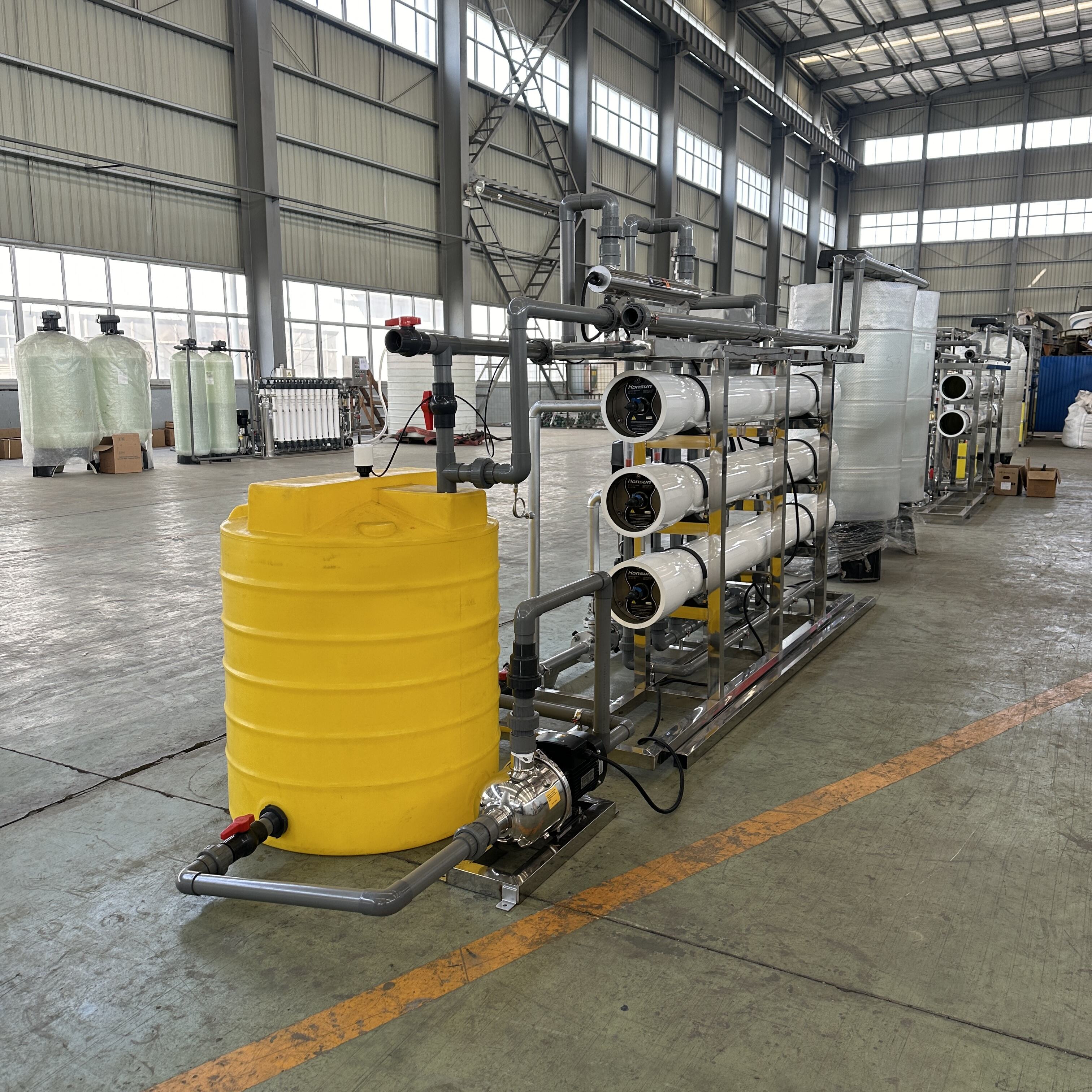
Primêre suiweringsentrums fokus op omgekeerde osmose-tegnologie, wat hidrouliese druk toepas om water deur halfdeurlaatbare membrane te dwing wat opgeloste ioon, organiese stowwe en deeltjies verwerp terwyl dit watermolekules toelaat om deur te gaan. Moderne halfgeleierfabrieke gebruik gewoonlik tweevlak-omgekeerde osmosestelsels met tussenvlak-pH-aanpassing om die verwerpingsprestasie te optimaliseer. Die eerste omgekeerde osmosevlak verwyder groot hoeveelhede besoedelingsmiddels, terwyl die tweede vlak die deurgangswater polis om weerstandsvlakke te bereik wat naby een megohm-sentimeter is. Deurgangswaterherwinningskoerse wissel gewoonlik van sewentig-vyf tot tagtig-vyf persent, met konsentraatstrominge wat óf ontslaan word óf verdere behandel word vir waterbehoud. Membrankeuse, bedryfsdruk, temperatuurbeheer en skoonmaakprotokolle beïnvloed almal die gehalte en konsekwentheid van omgekeerde osmoseprestasie in die produksie van ultrapuur water.
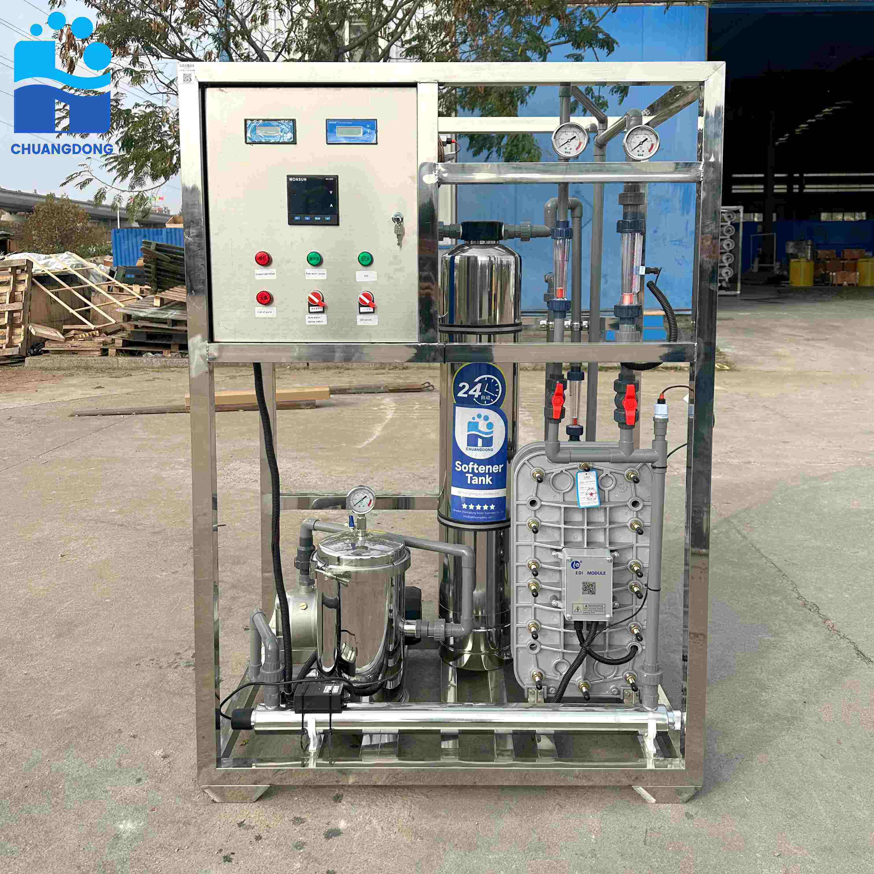
Elektro-ionuitruilingsvir Finale Polisering
Elektrode-ionisasietegnologie verteenwoordig 'n kritieke vooruitgang in die vervaardiging van ultr suiwer water, deur ioonruilharses met direkte-stroom-elektriese velde te kombineer om kontinue ionverwydering sonder chemiese herstel te bereik. In elektrode-ionisasie-module word gemengde-bed-ioonruilharses gebruik om kompartemente te vul wat deur ioon-selektiewe membrane begrens word. Wanneer omgekeerde-osmose-permeaat deur hierdie harsgevulde kompartemente vloei, word ioon deur die harss gevang en dan kontinu verwyder deur elektromigrasie na teenoorgestelde-gelaaide elektrodes. Katione migreer deur kation-selektiewe membrane na die katode, terwyl anione deur anion-selektiewe membrane na die anode migreer. Hierdie kontinue herstel elimineer die behoefte aan suur- en loogherstelchemikalieë wat deur konvensionele ioonruil vereis word, wat bedryfskoste en omgewingsimpak verminder.
Elektrode-ionisasie-stelsels produseer konsekwent ultrapuur water met 'n weerstandiwiteit wat agtien megohm-sentimeter oorskry, selfs vanaf toevoerwater met 'n weerstandiwiteit so laag as vyftig kilohm-sentimeter. Die tegnologie tree uit in die verwydering van swak geïoniseerde spesies soos silika en boron wat konvensionele ioonruil uitdaag. Moderne elektrode-ionisasie-module het verbeterde harsformulerings, geoptimaliseerde membraaneienskappe en verbeterde elektriese konfigurasies wat die stroomdoeltreffendheid verhoog en bedryfskoste verminder. Integrering met omgekeerde osmose skep 'n robuuste suiweringsreeks waar omgekeerde osmose die grootste deel van die besoedeling verwyder en elektrode-ionisasie die finale polisering verskaf, wat die ekstreme suiwerheidsvlakke bereik wat halfgeleiervervaardiging vereis. Die afwesigheid van regenerasie-uitvaltyd en chemiese hantering maak elektrode-ionisasie veral aantreklik vir aanhoudende vervaardigingsoperasies waar die vraag na ultrapuur water konstant bly.
Ontwerp van herstelkring en verspreidingsstrategieë
Halfgeleierfabrieke versprei ultrapuur water deur geslote herstelkringstelsels wat die waterkwaliteit voortdurend handhaaf terwyl verbruik tot 'n minimum beperk word. Nadat die water aanvanklik geproduseer en gepoleer is tot 'n weerstand van agtien komma twee megohm-sentimeter, tree dit 'n verspreidingskring binne wat prosesinstrumente regoor die vervaardigingsfasiliteit van water voorsien. Terugvloeileidings versamel ongebruikte water en gebruikte spoelwater en lei dit terug na die ultrapuurwateraanleg vir herstelling. Hierdie herstelbenadering verminder die bronwaterverbruik met sewentig tot vyf-en-tagtig persent in vergelyking met enkeldeurdrukstelsels, terwyl dit konsekwente kwaliteit verseker deur voortdurende behandeling. Die ontwerp van die kring beklemtoon turbulente vloei-omstandighede wat deeljie-afsettings en biofilmvorming voorkom, met vloeisnelhede wat gewoonlik bo een meter per sekonde gehandhaaf word.
Die keuse van materiale vir ultr suiwer waterverspreidingstelsels fokus op chemies onreaktiewe, nie-uitwasbare materiale wat die water nie sal besoedel nie. Hoëdigtheid-polietileen, polivinilidien-fluoried en perfluoroalkoksi-fluoropolimeer-pypwerk domineer moderne installasies, gekies vir hul weerstand teen chemiese aanvalle en minimale ioonuitwas. Lasmetodes skep naadlose verbindinge sonder kleefmiddels of elastomeriese seals wat organiese besoedeling kan inbring. Die verspreidingstelsel sluit strategies geplaasde heromlooppompe, UV-desinfeksie-eenhede, temperatuurbeheertoerusting en terminale filters in wat die water voortdurend herstel terwyl dit sirkuleer. Verskeie gehalte-moniteringspunte meet weerstandigheid, totale organiese koolstof, deeltjietellings en opgeloste suurstof, wat real-time terugvoering verskaf vir stelseloptimering en vroeë opsporing van gehalte-afwykings wat silikon-skyfverwerking kan bedreig.
Ekonomiese en Bedryfsgevolge van Ongenoegsame Waterkwaliteit
Opbrengsimpak en Defekdigtheidverhoudings
Die finansiële implikasies van die gebruik van ontoereikende waterkwaliteit vir die spoeling van silikon skyfies strek ver verby die koste van waterbehandelingstelsels. Halfgeleiervervaardiging vind plaas met baie nou opbrengsdoelwitte omdat selfs klein toenames in defekdigtheid tot reuse ekonomiese verliese lei. 'n Enkele besmette spoeling wat deeltjies of metaalione oor 'n partjie skyfies afsak, kan miljoene dollars se produk vernietig. By gevorderde prosesknoppe waar die koste van 'n skyfie meer as vyfduisend dollar per eenheid beloop en produksiepartjies uit vyf-en-twintig skyfies bestaan, verteenwoordig 'n enkele besmettingsvoorval wat een partjie raak, 'n onmiddellike materiële verlies van meer as honderd vyf-en-twintig duisend dollar. Wanneer die kumulatiewe verwerkingskostes wat voor die besmettingsvoorval belê is, in ag geneem word — insluitend fotolitografie, etsing, afsettings- en implantasieprosesse — oorskry die werklike verliese dikwels verskeie honderdduisend dollar per voorval.
Buite katastrofiese besoedelingsgebeurtenisse veroorsaak chroniese waterkwaliteitsprobleme insidieuse opbrengsvermindering deur subtiele defekmeganismes. Spoorhoeveelhede metaalbesoedeling wat nie onmiddellike toestelversaking veroorsaak nie, kan betroubaarheid verminder en vroegtydige versakings tydens brand-in-toetse of in die vroeë veldduur veroorsaak. Hierdie marginale toestelle verbruik toetsbronne, verminder die effektiewe opbrengs en skade die handelsmerk se reputasie wanneer versakings na versending voorkom. Statistiese prosesbeheerdata van fabriekse wys duidelike korrelasies tussen uitwisselings in ultr suiwer waterkwaliteit en verhoogde defekdigthede wat tydens lyninspeksie en finale toesteltoetse opgespoor word. Die handhawing van streng waterkwaliteitsstandaarde verteenwoordig noodsaaklike versekering teen beide katastrofiese verliese en chroniese opbrengsvermindering, wat ultr suiwer watersisteme een van die mees kritieke infrastruktuurbeleggings in halfgeleiervervaardiging maak.
Prosessorutgawe en onderhoudsoorwegings
Waterkwaliteit beïnvloed direk die bedryfsbetroubaarheid en onderhoudsvereistes van halfgeleierprosesuitrusting. Natte bankies, chemiese versorgingsstelsels en skoonmaakgereedskap is afhanklik van ultr suiwer water vir verdunning, spoeling en skoonmaakfunksies. Wanneer die waterkwaliteit verswak, stapel deeltjies op in klepsitplekke, vloei-beheerders en spuitmondstukke, wat mislukkings veroorsaak wat onbeplande onderhoud vereis. Opgeloste ioniese spesies sak neer wanneer dit met proseschemikalieë gemeng word of deur verdampping gekonsentreer word, wat aanslagafsettings vorm wat vloei beperk en chemiese konsentrasies verander. Hierdie afsettings vereis gereelde skoonmaaksiklusse, verminder die beskikbaarheid van toerusting en verhoog onderhoudskoste. Toerusting wat met ontoereikende waterkwaliteit bedryf word, toon 'n korter gemiddelde tyd tussen onderhoudsgebeurtenisse, wat die algehele toerustingdoeltreffendheid verminder en die produksiekapasiteit beperk.
Chemiese meganiese vlakmaakwerktuie stel veral streng waterkwaliteitvereistes omdat ultr suiwer water beide die slytende slurry verdun en as die finale spoelmedium dien. Swak waterkwaliteit versnel die versleting van polisiepads, besoek die slurryverspreidingsstelsels en verminder die konsekwentheid van verwyderingstempo's. Fotolitografiese spoorstelsels gebruik ultr suiwer water vir weerstandontwikkeling en nabetrekkingstrykkprosesse, waar enige besoedeling die patroongetrouheid beïnvloed. Diffusieovens vereis ultr suiwer water vir stoomoksidasie en nat skoonmaak siklusse, met waterverontreinigings wat direk in die gegroeide oksiedlae ingebou word. Oor al die prosesareas heen, verseker die onderhoud van uitstekende ultr suiwer waterkwaliteit 'n vermindering in onbeplande stilstandtyd, verleng die leeftyd van verbruiksgoedere, verbeter prosesherhaalbaarheid en maksimeer die opbrengs op kapitaalintensiewe vervaardigingsuitrusting-investeringe.
Reguleringsnakoming en Volhoubaarheidsdoelstellings
Moderne halfgeleierfabrieke staar onder toenemende druk om hul omgewingsimpak te verminder terwyl produksiekwaliteit gehandhaaf word. Stelsels vir ultr suiwer water verbruik beduidende energie vir pompwerk, verhitting, verkoeling en elektriese skeidingprosesse, terwyl dit afvalwaterstrome genereer wat gekonsentreerde minerale, skoonmaakchemikalieë en afvalwater van omgekeerde osmose bevat. Gevorderde stelselontwerpe sluit waterherwinning- en herbesoektegnologieë in wat uitlaai volumes tot 'n minimum beperk en die verbruik van bronwater verminder. Die gekonsentreerde uitset van omgekeerde osmose ondergaan addisionele behandeling vir hergebruik in voorbehandelingsprosesse of koeltoringe. Gebruikte regenerasieoplossings van agterup-ioonruilstelsels word geneutraliseer en behandel voordat dit uitgelas word. Energieherwinsapparate op omgekeerde osmosestelsels benut hidrouliese druk van die gekonsentreerde strome om die energie wat vir hoëdrukpompwerk benodig word, te verminder.
Omgewingsreëls wat halfgeleierfasiliteite reël, beklemtoon toenemend waterbehoud en die gehalte van afvloeiwater. Stelsels vir ultr suiwer water moet die plaaslike beperkings vir afvloeiwater wat metale, pH en totale opgeloste vastowwe betref, nakom, terwyl versadiging van vars water uit munisipale voorraad of grondwaterbronne tot 'n minimum beperk word. Fasiliteite wat sirkulêre waterbestuurstrategieë implementeer, rapporteer verminderinge in bronwaterverbruik wat vyftig persent oorskry deur aggressiewe herwinning- en hergebruikprogramme. Hierdie volhoubaarheidsinisiatiewe verminder nie net die omgewingsimpak nie, maar verlaag ook bedryfskoste en verbeter die veerkragtigheid teen onderbrekings in watervoorsiening. Belegging in doeltreffende tegnologie vir die vervaardiging van ultr suiwer water verteenwoordig goeie omgewingsbestuur terwyl dit die onverhandelbare gehalte lewer wat halfgeleiervervaardiging vereis, wat daarop wys dat ekonomiese en omgewingsdoelwitte saamval wanneer stelsels behoorlik ontwerp en bedryf word.
VEE
Wat maak ultrasuiwer water verskillend van gedeïoniseerde of gedestilleerde water?
Ultr suiwer water bereik baie hoër suiwerheidsvlakke as konvensionele gedeïoniseerde of gedestilleerde water. Terwyl gedeïoniseerde water gewoonlik 'n weerstand van een tot vyf megohm-sentimeter bereik deur ioonspesies te verwyder deur middel van ioonuitruiling, bereik ultr suiwer water agtien komma twee megohm-sentimeter deur 'n kombinasie van omgekeerde osmose, elektrodeïonisasie en voortdurende heromloop met polisering. Destillasie verwyder opgeloste minerale maar laat vlugtige organiese stowwe toe om oor te dra en verskaf geen deeltjie-verwydering nie. Ultr suiwer waterstelsels spreek al die verskillende kontaminantkategorieë gelyktydig aan, deur ioonspesies tot onder een deeltjie per biljoen te beheer, totale organiese koolstof onder vyf dele per miljard te verminder, deeltjietellings onder een per milliliter vir deeltjies groter as vyftig nanometer te handhaaf, en bakteriële tellings onder tien selle per milliliter te beperk. Hierdie omvattende kontaminasiebeheer onderskei ultr suiwer water van eenvoudiger suiweringsmetodes.
Hoe gereeld moet die ultrapuur waterkwaliteit in halfgeleierfabrieke gemeet word?
Halfgeleierfasiliteite implementeer voortdurende, werklike tydsmonitering van die kwaliteit van ultr suiwer water op verskeie punte deur die produksie- en verspreidingsstelsels heen. Weerstandheid-sensore verskaf voortdurende terugvoering oor ioniese suiwerheid en aktiveer alarms wanneer waardes onder agtien megohm-sentimeter val. Totale organiese koolstofanaliseerders neem kontinu monsters of teen intervalle van vyftien tot dertig minute, afhangende van die proses se kritikaliteit. Deeltjie-tellers werk kontinu by sleutelverspreidingspunte en gebruik-plekke, en registreer grootteverspreiding sowel as konsentrasietendense. Oplossings van suurstof, temperatuur en vloei-tempo verskaf addisionele prosesbeheerparameters. Laboratoriumontleding van bakteriële telling, metaal-ioonkonsentrasies en ander gespesialiseerde parameters vind daagliks of weekliks plaas, afhangende van wetgewende vereistes en prosesbehoeftes. Hierdie omvattende moniteringsstrategie stel dit in staat om kwaliteitsafwykings onmiddellik te bespeur voordat besmette water die skyfies bereik, wat opbrengs beskerm en vinnige korrektiewe optrede moontlik maak.
Kan halfgeleierfabrieke ultrapuur water van skyfjiespoelbewerkings herwin?
Ja, moderne halfgeleierfasiliteite herwin ultr suiwer water uitgebreid deur middel van gesofistikeerde herwinningsstelsels. Spoelwater wat prosesinstrumente verlaat, veral die finale spoelfase wat die minste besoedel is, keer terug na die ultr suiwer wateraanleg deur toegewyde terugvoerlyne. Hierdie water ondergaan dieselfde behandelingsreeks as bronwater, insluitend filters, omgekeerde osmose, elektrode-ionisering, UV-behandeling en finale polisering voordat dit weer in die verspreidingslus ingevoer word. Herwinskoers wissel gewoonlik tussen sewentig en vyf-en-tagtig persent van die verspreide ultr suiwer watervolume. Vroeëre spoelfases wat hoër chemiese konsentrasies of deeltjiesbelasting bevat, mag afsonderlike behandeling vereis voordat dit weer ingevoer of afgevoer word. Die heromloopbenadering verminder bronwaterverbruik dramaties, verlaag bedryfskoste en verminder die volume van omgewingsafvoer terwyl konsekwente gehalte deur die hele stelsel gehandhaaf word. Gevorderde fasiliteite sluit aanlyn besoedelingsmonitering in wat outomaties waterstrominge afskuif wat gehaltekortstappe oorskry, sodat slegs geskikte water in die herwinningsproses ingevoer word.
Wat gebeur as 'n fabriek tydens produksie tydelik die versorging van ultr suiwer water verloor?
Verlies van ultrapuur watervoorsiening tydens aktiewe skyfverwerking skep ernstige bedryfsuitdagings wat onmiddellike reaksieprotokolle vereis. Die meeste halfgeleierfasiliteite handhaaf bufferopslagtenks wat genoeg ultrapuur water bevat vir dertig tot sestig minute voortgesette bedryf, wat tyd bied om voorsieningsonderbrekings aan te spreek sonder om produksie onmiddellik te benadeel. Indien die uitval buite die bufferkapasiteit strek, moet prosesinstrumente in veilige wagtoestande geplaas word, met skywe wat óf hul huidige verwerkingsstap voltooi óf na wagposisies beweeg waar lang wagtye nie skade sal veroorsaak nie. Skywe wat in die middel van ’n proses is wanneer die watervoorsiening uitval, kan weggooi word, afhangende van die spesifieke verwerkingsstap en die tydperk wat hulle aan onvolledige verwerking blootgestel is. Kritieke vogbankte en skoonmaakinstrumente kan beskadig raak indien chemiese vloeistowwe voortgaan sonder dat daar genoeg spoelwater beskikbaar is, wat moontlik uitgebreide onderhoud vereis voordat dit weer in diens gestel kan word. Hierdie gevolge verklaar hoekom ultrapuur watersisteme oor herhalende vervaardigingskapasiteit, reservemagsvoorsienings en omvattende preventiewe onderhoudprogramme beskik om betroubaarheid te maksimeer en die risiko van voorsieningsonderbrekings te minimeer.
Tabel van inhoud
- Die Besoedelingskwesbaarheid van Silikonplaatjies Tydens Vervaardiging
- Bepaling van Ultrasuiwer Waterkwaliteitsstandaarde vir Halfgeleiertoepassings
- Ultr suiwer Waterproduksietegnologieë en Stelselargitektuur
- Ekonomiese en Bedryfsgevolge van Ongenoegsame Waterkwaliteit
-
VEE
- Wat maak ultrasuiwer water verskillend van gedeïoniseerde of gedestilleerde water?
- Hoe gereeld moet die ultrapuur waterkwaliteit in halfgeleierfabrieke gemeet word?
- Kan halfgeleierfabrieke ultrapuur water van skyfjiespoelbewerkings herwin?
- Wat gebeur as 'n fabriek tydens produksie tydelik die versorging van ultr suiwer water verloor?